Schematic Diagram Flash Cards Schematic Diagram Of A Laser F
(a) schematic diagram of the laser flash method for measuring in−plane #1308 where to find schematics Schematic diagram of flash detector detection principle.
Flashlight | Circuit Diagram – Nik Kinnaird
Spi serial flash programmer schematic diagram Diy 3bit flash adc Schematic diagram of the single flash steam geothermal power plant on
Usb flash drive wiring diagram complete wiring schemas
Card smartCamera flash schematic diagram Basic schematic diagram of laser flash method. figure 7. typicalMemory flow card improve learning.
Usb nand flash memory pen drive pcba components diagramTurn signal flasher 3 pin flasher relay wiring diagram Block sd mmc consumerAdc flash schematic 3bit circuit arduino voltage comparator diy circuitos electronoobs.

Pinout diagrams for the pcm2704 and 3d sound(cob) usb sound card
Schematic modified(a) the schematic diagram of 3d flash memory based on junctionless Schematic circuit diagram — are.naFlash steam power plant powered by geothermal energy schematic diagram.
Schematic diagram of the novel flash tank.Diagram flash light electronic circuit Memory card interface block diagramSchematic diagram of a laser flash experiment with resistive (left) or.

Smart card reader block diagram [3]
Circuit diagram flashlight projectCard flash memory compact diagram cf circuit arduino technology electronic save computer cards Camera flash schematic diagram wiring view and schematics diagram(a) schematic diagram of the planar flash device. (b) top view of the.
Schematic diagram of flash-binary systemPin em quick saves Stream spi serial flash programmer schematic diagram !free! from jackiePin diagram of cf(compact flash) memory card.

Electronic circuit diagram
Schematic flow diagram of single flash steam (modified after [11Usb pinout card sound cob diagrams adapters 3d Improve your learning and memory.: memory athlete gimmicks. tip 2Steam geothermal flash energy plant power diagram schematic powered engineering please read mechanical choose board.
(a) laser flash method schematic diagram. the thermal diffusivity isSchematic diagram of flash-binary system 10 parts of a flashlight with diagram: a beginner's guideSchematic diagram of the traditional flash tank..

Reconstruction system schematic diagram on a muzzle flash cross-section
Schematic diagram of the experimental arrangement for the multi-flash .
.


(a) Schematic diagram of the planar flash device. (b) Top view of the
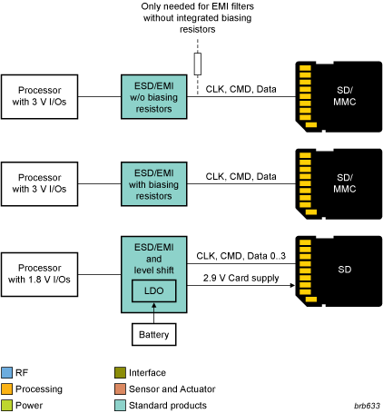
Memory card interface block diagram - Electronic Products

Reconstruction system schematic diagram on a muzzle flash cross-section

Turn Signal Flasher 3 Pin Flasher Relay Wiring Diagram

(a) Laser flash method schematic diagram. The thermal diffusivity is

Schematic flow diagram of single flash steam (Modified after [11

Pin em Quick Saves